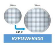
R2POWER300
Preparing R2 extension to 300mm for BCD Smart Power and Power Discretes

 |
R2POWER300 Preparing R2 extension to 300mm for BCD Smart Power and Power Discretes |
 |
Journal papers
1) C. Cozzi, G. Polito, K. Kolasinski, G. Barillaro, Controlled Microfabrication of High-Aspect-Ratio Structures in Silicon at the Highest Etching Rates: The Role of H2O2 in the Anodic Dissolution of Silicon in Acidic Electrolytes, Advanced Functional Materials, 27, 1604310 (2017)
2) S. Vangelista, Rossella Piagge, Satu Ek, Tiina Sarnet, Gabriella Ghidini and Alessio Lamperti, Structural, Chemical and Optical Properties of Cerium Dioxide Film Prepared by Atomic Layer Deposition on TiN and Si Substrates, Thin Solid Films, DOI: 10.1016/j.tsf.2017.05.034
3) G. Polito, C. Cozzi, G. Barillaro Controlling the Electrochemical Etching of Pores with High Aspect Ratio at the Submicrometer Scale in Silicon, ECS Transactions, Vol. 77, No. 5, pp. 259-266, 2017.
4) C. Cozzi, G. Polito, K. W. Kolasinski, G. Barillaro Controlled Fabrication of High Aspect Ratio Microstructures in Silicon at Etching Rates Beyond State of the Art Microstructuring Technologies, ECS Transactions, Vol. 77, No. 5, pp. 199-206, 2017.
5) A.N. Tallarico, , S. Reggiani , P. Magnone , G. Croce , R. Depetro , P. Gattari, E. Sangiorgi, C. Fiegna, Investigation of the hot carrier degradation in power LDMOS transistors with customized thick oxide, Microelectronics Reliability, Vol. 77, special issue 28th European Symposium on Reliability of Electron Devices, Failure Physics and Analysis, 2017, Pages 475-479
6) Andrea Tallarico, Susanna Reggiani, Riccardo Depetro, Andrea Mario Torti, Giuseppe Croce, Enrico Sangiorgi, Claudio Fiegna, Hot-Carrier Degradation in Power LDMOS: Selective LOCOS- Versus STI-Based Architecture, IEEE Journal of the Electron Devices Society ( Volume: 6 ), pp.219 - 226, DOI 10.1109/JEDS.2018.2792539 OPEN ACCESS
7) L. M. Strambini, C. Cozzi, and G. Barillaro, Quasi-Zero-Voltage Controlled Etching Of Macropores in n-Type Silicon, ECS Transactions, 85 (6) 93-95 (2018) DOI: 10.1149/08506.0093ecst
8) Silvia Vangelista, Rossella Piagge, Satu Ek and Alessio Lamperti, Beilstein J. Effect of annealing treatments on CeO2 grown on TiN and Si substrates by atomic layer deposition, Nanotechnol. 2018, 9, 890–899. doi:10.3762/bjnano.9.83 PLATINUM OPEN ACCESS [ST, CNR, PICOSUN]
9) S. Reggiani, M. Rossetti, A.N.Tallarico, A.Molfese, S.Manzini, R.Depetro, G.Croce, E.Sangiorgi, C.Fiegna "TCAD investigation on hot-electron injection in new-generation technologies", Microelectronics Reliability, Volumes 88–90, September 2018, Pages 1090-1093, doi:10.1016/j.microrel.2018.07
Conference presentations
1) Tommi Suni and Satu Ek ALD for MEMS, MEMSWAVE, 4-6th July, 2016, Romania.
2) Riina Ritasalo, Kestutis Grigoras, Satu Ek, Tero Lehto, Erik Østreng, Tero Pilvi, Alexey Veselov, High aspect ratio structures deposited by ALD for 3D applications, 16th International Conference on Atomic Layer Deposition, 24th-27th July 2016, Dublin, Ireland, www.ald2016.com
3) Riina Ritasalo, Kestutis Grigoras, Satu Ek, Tero Lehto, Erik Østreng, Tero Pilvi, Alexey Veselov, High aspect ratio structures deposited by ALD for 3D applications. Baltic Conference on Atomic Layer Deposition (BALD) , 2-4th Oct., 2016, St. Petersburg Russia, www.bald2016.ru
4) M. Scurati, R2POWER300 European Nanoelectronic Forum – Rome 23, 24 November 2016
5) S. Ek, R. Ritasalo, T. Sarnet, J. Kalliomäki, E. Østreng, S. Vangelista, A. Lamperti, R. Piagge, G.Ghidini, High-k RE oxide ALD films characterized by SEM and electrical techniques, 17th International Conference on Atomic Layer Deposition, 15th-18th July 2017, Denver, Colorado, US, aldconference.avs.org
6) S. Ek, R. Ritasalo, T. Sarnet, J. Kalliomäki, E. Østreng, S. Vangelista, A. Lamperti, R. Piagge, G.Ghidini High-k RE oxide ALD films characterized by SEM and electrical techniques, Joint EUROCVD-21-Baltic ALD-15, 11th-14th June 2017, Linköping, Sweden, www.eurocvd-balticald2017.se
6) S. Vangelista, Rossella Piagge, Satu Ek, Tiina Sarnet, Gabriella Ghidini and Alessio Lamperti, Structural Properties of Cerium Dioxide Film Prepared by Atomic Layer Deposition on TiN and Si Substrates - 2017 MRS Spring Meeting, April 17-21, 2017 in Phoenix, Arizona - Symposium: ED7: Materials and Device Engineering for Beyond the Roadmap Devices in Logic, Memory, and Power.
7) M. Scurati, R2POWER300, Ecsel JU Symposium, 13, 14 June 2017, Porto Maso, St. Julian's, Malta.
8) A.N. Tallarico, S. Reggiani, P. Magnone, G. Croce, R. Depetro, P. Gattari, E. Sangiorgi, C. Fiegna, Investigation of the hot carrier degradation in power LDMOS transistors with customized thick oxide accepted for èresentation, ESREF 2017
11) Controlled Fabrication of High-Aspect-Ratio Microstructures in Silicon at Etching Rates Beyond State-of-the-Art Microstructuring Technologies C. Cozzi, G. Polito (University of Pisa), K. W. Kolasinski (West Chester University), and G. Barillaro (University of Pisa 231st ECS Meeting, New Orleans (USA), May 28 - June 1st, 2017
10) Controlling the Electrochemical Etching of Pores with High Aspect Ratio at the Submicrometer Scale in Silicon G. Polito, C. Cozzi, and G. Barillaro (University of Pisa) 231st ECS Meeting, New Orleans (USA), May 28 - June 1st, 2017
11) A. Lamperti, S. Vangelista, R. Piagge, R. Ritasalo, T. Sarnet, CeO2 thin films deposited by ALD on Si or TiN: can the initial growth steps explain the crystalline orientation?, 2017 E-MRS Fall Meeting and Exhibit, Symposium on Synchrotron radiation and atomic layer deposition for advanced materials, Warsaw University of Technology, September 18-21 (oral presentation). [ST, CNR, PICOSUN]
12) S. Vangelista, S. Ek, T. Sarnet, R. Piagge, G. Ghidini and A. Lamperti, Structural properties of Cerium dioxide film prepared by atomic layer deposition on TiN and Si substrates, 2017 E-MRS Fall Meeting and Exhibit, Symposium on Advanced oxide materials – growth, characterization and applications, Warsaw University of Technology, September 18-21 (poster presentation). [ST, CNR, PICOSUN] 13) Lucanos M Strambini , Chiara Cozzi and Giuseppe Barillaro, Quasi-Zero-Voltage Controlled Etching of Macropores in n-Type Silicon, 223rd Meeting Electrochemical Society 2018, MA2018-01 1386.
14) S. Vangelista, R. Piagge, S. Spadoni, E. Ravizza, G. Ghidini, I. Rossetto, F. Toia, R. Ritasalo, P. Jarvinen and A. Lamperti, Structural and chemical changes in nanoscaled La2O3/CeO2stacks under different annealing treatments, ECOSS 34th Session on Oxide surfaces and thin films (OXI) 26-31 August 2018, Aarhus, Denmark (oral contribution). [ST, CNR, PICOSUN]
15) I.Rossetto, R.Piagge, F.Toia, S.Spiga, A.Lamperti, S.Vangelistai, R. Ritasalo, P. Jarvinen and G.Ghidini, Impact of annealing on the current conduction and trap properties of CeO2/La2O3 Metal Insulator Metal capacitors, WODIM 2018 - 20th Workshop on Dielectrics in Microelectronics, June 10-14, 2018 Berlin, Germany (oral presentation). [ST, CNR, PICOSUN]
16) R. Piagge, S. Spadoni, S. Vangelista, E. Ravizza, G. Ghidini, R. Ritasalo, P. Jarvinen and A. Lamperti, Evaluation of structural and chemical properties of La2O3/CeO2 stacks by atomic layer deposition under in-situ annealing, MAM2018 27th Materials for Advanced Metallization Conference, Milano, March 18-21 2018 (poster presentation). [ST, CNR, PICOSUN]
17) European ECSEL Project Results & Demonstrators - JUNE 13rd 2018- Minatec Grenoble [ST, LPE]
18) ECSEL JU Symposium 19, 20 June 2018, Bruxelles [ST]
19) S. Reggiani, M. Rossetti, A.N.Tallarico, A.Molfese, S.Manzini, R.Depetro, G.Croce, E.Sangiorgi, C.Fiegna "TCAD investigation on hot-electron injection in new-generation technologies", 29th European Symposium on Reliability of Electron Devices, Failure Physics and Analysis ( ESREF 2018 ).
Exhibitions
Semicon Show, Grenoble, 26 October 2016 (Besi-NL)
SMT Hybrid Packaging 2017, Nuremberg, 18 May 2017 (Besi-NL)
Dissemination through Master and PhD Courses
Electronic Technologies for Energy and Information Technology, Master Course "Electronics and Telecommunications Enegineering for Energy", University of Bologna (IUNET)
Ph.D. Course: Marco Morelli, STMicroelectronics - Italy, “Semiconductor trip: from a simple idea to a complex manufacturing”, PhD in Information Engineering, Information Engineering Dpt, University of Pisa, 19-23 june 2017 (total teaching hours: 27)
Ph.D. Course: Marco Morelli et al., STMicroelectronics - Italy, “Semiconductor trip: from a simple idea to a complex manufacturing”, PhD in Electronics, Telecommunications and Information Technology Engineering, DEI, University of Bologna, 11-15 June 2018.